ADN8810
Rev. A | Page 5 of 16
TIMING CHARACTERISTICS
1, 2
Table 2. Timing Characteristics
Parameter
Description
Min
Typ
Max
Unit
fCLK
SCLK Frequency
12.5
MHz
t
1
SCLK Cycle Time
80
ns
t2
SCLK Width High
40
ns
t3
SCLK Width Low
40
ns
t
4
CS
15
Low to SCLK High Setup
ns
t
5
CS
15
High to SCLK High Setup
ns
t6
SCLK High to
CS
35
Low Hold
ns
t
7
SCLK High to
CS
20
High Hold
ns
t
8
Data Setup
15
ns
t9
Data Hold
2
ns
t10
CS
30
High Pulsewidth
ns
t
11
RESET
40
Pulsewidth
ns
t12
CS
High to
30
RESET
Low Hold
ns
NOTES
1
Guaranteed by design. Not production tested.
2
Sample tested during initial release and after any redesign or process change that may affect these parameters. All input signals are measured with tr = tf = 5 ns (10%
to 90% of DVDD) and timed from a voltage level of (VIL + VIH)/2.
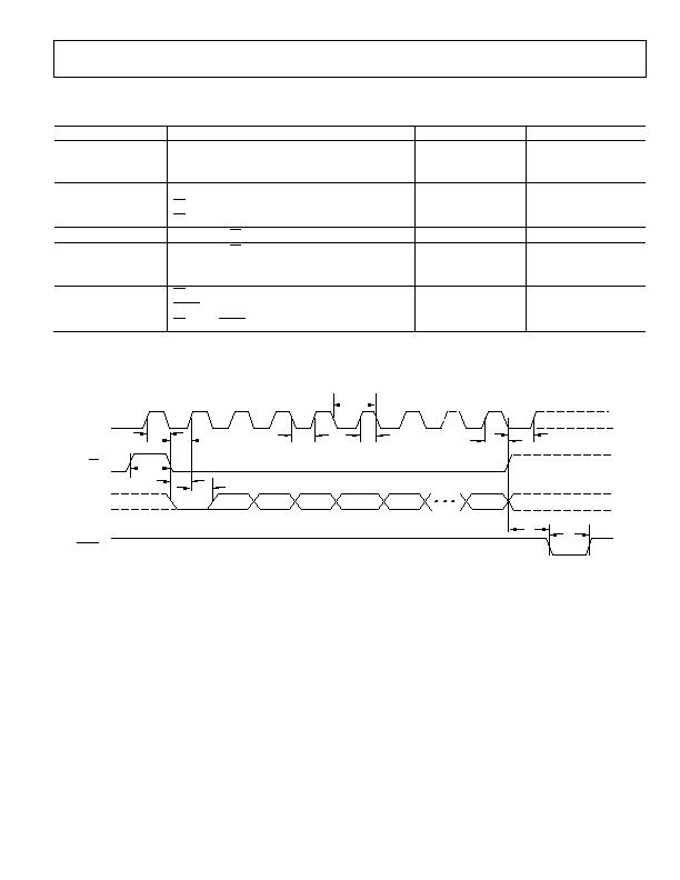
SCLK
CS
SDI
t
6
t
4
t
3
t
2
t
7
t
5
t
1
t
10
t
8
t
9
A3*
A2
t
12
t
11
A1
A0
D11
D10
D0
ESET
*ADDRESS BIT A3 MUST BE LOGIC LOW
Figure 2. Timing Diagram
发布紧急采购,3分钟左右您将得到回复。
相关PDF资料
ADP2140ACPZ3328R7
IC REG DL BCK/LINEAR 10LFCSP
ADP5022ACBZ-6-R7
IC REG TRPL BCK/LINEAR 16WLCSP
ADP5041ACPZ-1-R7
IC REG TRPL BCK/LINEAR 20-LFCSP
ADP5042ACPZ-2-R7
IC REG TRPL BCK/LINEAR 20LFCSP
ADT6402SRJZ-RL7
IC TEMP SENS TRIP PT PP SOT-23-6
ADT6501SRJZP085RL7
IC TEMP SENSOR MICROPWR SOT23-5
ADT7302ARTZ-500RL7
IC SENSOR TEMP 13BIT DGT SOT23-6
ADT7310TRZ
IC TEMP SENSOR 16BIT SPI 8SOIC
相关代理商/技术参数
ADN8810-EVAL
制造商:Analog Devices 功能描述:- Bulk
ADN8810XCP
制造商:Analog Devices 功能描述:- Bulk
ADN8820
制造商:Analog Devices 功能描述:LASER DRVR 1CH 48LFCSP - Trays
ADN8820ACP
制造商:Analog Devices 功能描述:LASER DRVR 1CH 48LFCSP - Bulk
ADN8820-REEL7
制造商:AD 制造商全称:Analog Devices 功能描述:EDFA and CW Laser Controller
ADN8830
制造商:AD 制造商全称:Analog Devices 功能描述:Thermoelectric Cooler Controller
ADN8830ACP
制造商:Analog Devices 功能描述:Temp Sensor Digital 32-Pin LFCSP EP 制造商:Rochester Electronics LLC 功能描述:HIGH PRECISION/EFFICIENCY TEC CONTROLLER - Bulk
ADN8830ACP-REEL
制造商:Analog Devices 功能描述:Temp Sensor Digital 32-Pin LFCSP EP T/R
